
NIST Researchers Develop Photonic Chip Packaging That Can Withstand Extreme Environments
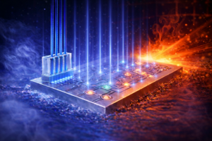
Researchers at the National Institute of Standards and Technology (NIST) have developed a new way to package photonic integrated circuits — chips that transmit information with light instead of electricity — so they can operate in some of the harshest environments imaginable, from deep-space probes to nuclear reactors. The technique adapts a method called hydroxide catalysis bonding (HCB), originally pioneered by NASA, to create a glasslike, inorganic bond between optical fibers and the chip, replacing conventional polymer adhesives that tend to crack, drift or degrade under extreme temperature swings, vacuum and radiation. For manufacturers and technology developers, this opens the door to using high-speed, low-power photonic chips in applications that demand exceptional reliability under punishing conditions.
To validate the approach, NIST scientists subjected HCB-packaged photonic chips to cryogenic temperatures, rapid thermal cycling, high vacuum and intense ionizing radiation, confirming that the fiber-to-chip connection stayed aligned and the devices continued to function normally. Additional tests showed the bonded assemblies remain mechanically stable at temperatures far beyond the limits of standard adhesives, suggesting strong potential for industrial, energy and quantum systems that must operate across wide environmental ranges. Although the current bonding process takes several days, the team emphasizes that this is an engineering challenge that can be streamlined for manufacturing, positioning the technique as a promising foundation for robust, field-ready photonic packaging.
Read the entire article here.